![]()
|
|
|
Module#2:THE HANDYBOARD The handyboard is the heart of the rover, which contains important circuitry, the microcontroller, memory and allied devices. The handyboard is nothing but a PCB which is used in several amateur robotics projects. R ESEARCH AND RESULTSSeveral different circuit boards were considered for use on the rover. Among them were the miniboard and the 6.270 board. However we narrowed down our choice to the handyboard because it is more advanced than a mini-board and is more simplified as compared to a 6.270 board. COMPARING THE HANDY BOARD AND THE 6.270 BOARD SIMILARITIES
DIFFERENCES
Of all the microcontrollers researched upon, our microcontroller choice came down to two, the Motorola m68HC11 or the Intel 8051. When researching these microcontrollers, we discovered that 68HC11 had the following useful features.
The interfacing circuits that were chosen were present on a board known as the F1 Controller (also known as the Handy Board), an embedded controller based on the MC68HC11F1 microprocessor. It has been designed so that it can be configured for many diverse applications with the minimum of effort. It can be plugged directly into the serial port of a PC and allow us to talk to it and manipulate the I/O without having to write any programs, to test it. The Motorola HCMOS MC68HC11A1F4 is thus an advanced microcomputer containing highly sophisticated on-chip peripheral functions. An improved instruction set provides additional capability. The fully static design allows operation at frequencies down to DC, further reducing its already low power consumption.
Features available for the microcontroller are: 1) 512 bytes of EEPROM 2) 256 bytes of RAM 3) Enhanced 16 - bit timer system 4) A new serial peripheral interface 5) 8 channel 8-bit A/D converter 6) A real time interrupt circuit. It is a 52 pin IC. It has a DMA controller, internal clock generator, 2 interrupt request pins, 5 I/O ports viz. A,B,C,D,E. The I/P signal voltage given to the controller is 5Volts. OPERATING MODES: The MC68HC11A1FN uses 2 dedicated pins ( MODA & MODB) to select one of the two basic operating modes or one of the two special operating modes. The basic operating modes are Single-chip and Expanded multiplexed, and the special operating modes are Bootstrap and Special Test. Their selection is shown below:
We will be using the bootstrap mode only. In the bootstrap mode the bootloader, which is a program present in the EEPROM that contains all the vector addresses; reads a 256 byte program into the on-chip RAM. After this is done the control is automatically passed onto the program at memory address 0000. The O/P of the IR sensors and the shaft encoders are given to Port B and Pulse counter of the 6811 respectively. Now the 68HC11A1FN is programmed in such a way that it keeps checking the inputs at these two ports. The input from the shaft encoder is continuously added. Hence if the rover has to back a certain distance then the number of revolutions made by the wheel that has been counted using the shaft encoder can be found out by the timer count and thus the rover can move back by the same number of revolutions. Also if the sensors sense an obstacle then the output of the sensors will go low. Immediately the port to which the sensors are connected goes low and hence during status check the controller knows that there is an obstacle and it stops the rover by interrupting the motors connected to the wheel. These are the two main functions performed by the controller The Handy Board Block Diagram :
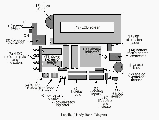
1. Power Switch. The power switch is used to turn the Handy Board on and off. The Handy Board retains the contents of its memory even when the board is switched off.2. Computer Connector. Via this RJ11 connector, the Handy Board attaches to a desktop computer (using the separate Interface/Charger Board).3. 4 DC Motor Outputs and Indicators. The Handy Board’s four motor outputs are located at this single 12–pin connector. Each motor output consists of three pins; the motor connects to the outer two pins and the center pin is not used. Red and green LEDs indicate motor direction.From top to bottom, the motor outputs are numbered 0 to 3. 4. Start Button. The Start button is used to control the execution of Interactive C programs. Also, its state may be read under user program control.5. Stop Button. The Stop button is used to put the Handy Board into a special bootstrap download mode. Also, its state may be read under user program control.6. Low Battery Indicator. The red Low Battery LED lights when for a brief interval each time the Handy Board is switched on. If this LED is on steadily, it indicates that the battery is low and that the CPU is halted.7. Power/Ready Indicator. The green Power/Ready LED lights when the Handy Board is in normal operation, and flashes when the Handy Board is transmitting serial data. If the board is powered on and this LED is off, then the Handy Board is in special bootstrap mode.8. 9 Digital Inputs. The bank of digital input ports is here. From right to left, the digital inputs are numbered 7 to 15.9. 7 Analog Inputs. The bank of analog input ports is here. From right to left, the analog inputs are numbered 0 to 6.10. IR Output and Indicator. The infrared output port is here. The red indicator LED lights when the output is enabled.11. IR Input Sensor. The dark green-colored infrared sensor is here.12. Analog Expansion Header. The analog expansion header is a 1_4 connector row located above analog inputs 0 to 3.13. User Knob. The user knob is a trimmer potentiometer whose value can be read under user program control.14. Battery Trickle-Charge Connector. The battery charge connector is a coaxial power jack to accept a 12 volt signal for trickle-charging the Handy Board’s internal battery.15. Charge Indicator. The yellow charge indicator LED lights when the Handy Board is charging via the coaxial power jack.16. SPI Expansion Header. The SPI expansion header is a 2_4 pin jack that allows connection with the 6811’s serial peripheral interface circuit. See the CPU and memory schematic diagram for a pin-out of this connector.17. LCD Screen. The Handy Board is provided with a 16_2 LCD screen which can display data under user control.18. Piezo Beeper. The Handy Board has a simple piezo beeper for generating tones under user control.19. Power Expansion Header. The power expansion header is a 1_4 pin jack that provides access to the power output from the serial expansion board.The Handy Board Circuit Diagram 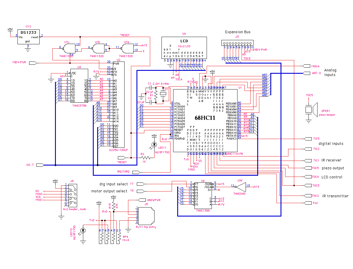
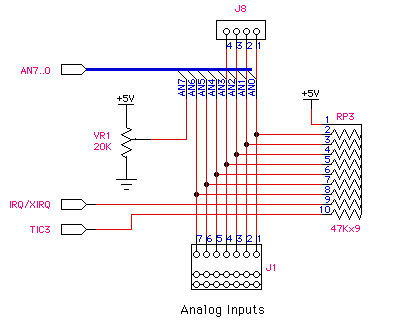
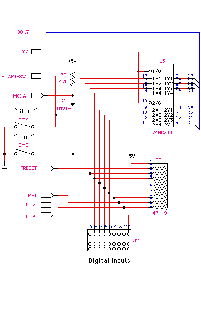
Click to view detailed diagram Circuit Working: The heart of the "rover" is the Motorola’s MC68HC11A1FN 8bit microcomputer. It is a single chip micro computer which contains highly sophisticated on-chip peripheral functions of 4K bytes of ROM ,512 bytes of EEPROM, 256 bytes of RAM, enhanced 16-bit timer system,8-BIT pulse accumulator circuit ,an enhanced non-return-to zero. Serial communications interface (SCI),a serial peripheral interface,8 channel 8_BIT A/D convertor etc: which help to drive the rover. The overall CPU and memory circuit consists of the controller, the RAM, the DS-1233 reset regulator, the quad Schmitt NAND gates, the 3 to 8 decoder, the LCD and the connectors for the various outputs viz: for the serial interface, LCD display, control outputs, multiplexed address data bus, the analog inputs, the buffer etc. The clock for the controller is provided by the oscillator ckt formed by C1, C2 and the 8-MHz crystal. The controller is used in the expanded multiplexed mode. The controller is made to work in bootstrapped mode to download the software into the RAM through serial communications interface. The port A has the lower 8-bits of address and the upper 8-bits are taken from port C which have multiplexed address data bus and are connected to the RAM through a buffer which latch the address or data depending upon "the address strobe " (AS) signal given by the controller. DS 1233 is a special reset power regulator chip which makes the controller OFF if it’s voltage level goes below the 4.5 V DC level. The 74HC138 is a 3 to 8 decoder which generally maps devices onto an address space. The enable inputs of decoder are important because they should not become active at the same time as RAM chip or else it would lead to "bus contention". Depending upon A13,A12 and the R/W signal, the O/P is selected which gives the O/P fromY0 to Y7.When the R/W signal is high,Y7 will be selected and the digital I/p’s from 74MC244 are activated. Similarly, for write operation Y6 the motor O/P’s would be selected. Controller gives the additional functions for various signals like for the IR receiver, the LCD control, the IR transmitter, piezo O/P etc:. Out of the 8 digital I/P’s two are for shaft encoder and four are for the sensors. Serial interface/battery charger: J11 is the coaxial power jack to which 12-15 Volts DC is given. It gives rectified output through LM2931Z-5.0 regulator which gives a 5Volt output. RJ 12 is the jack for supplying power to the handyboard as well as giving the signals. The battery charging can be done with the SW4 open and the fast charging is done with the help of "ZAP mode". The board communicates with the RS 232 system, but requires external circuitry to convert its own signals which obey digital logic norms to RS232 signals and this function is made possible by interfacing the MAX232 IC with the host computer. A DB 25 pin female connector makes the interface between the host computer and the serial interface board. Motor outputs: The L293D chip is the chip that incorporates two H-bridge motor driving circuits into a single 16-pin DIP package.8-BITS are used to control 4 motors.4 of the bits determine the direction of motors with the assistance of inverters and 4 bits determine whether the motors are ON or OFF. The data is latched and when Y6 the clock signal goes high depending on the data sent to the controller, signals are given to particular motor and cause corresponding movement of the body. The motor is powered by a battery source of 9.6 V. Depending upon the start SW, the corresponding LEDs glow which indicate the corresponding motion of a particular motor.
The Analog Input Circuit
The Digital Input Circuit |
|
1999 IEEE VESIT Student Branch Hits :
Webmaster : Saumitra Mohan Das |