![]()
|
|
|
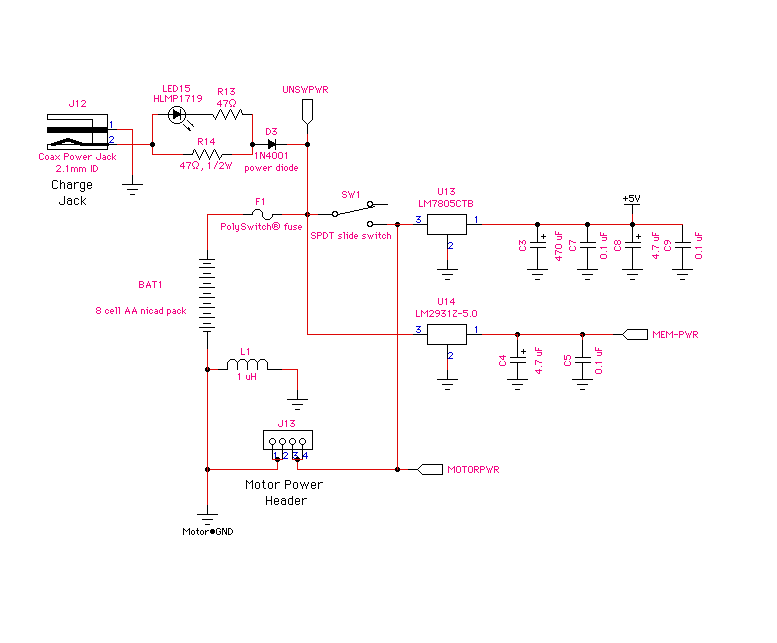
Module#5 : Serial Interface Board The serial interface board contains the RS 232 interface, and the power supply circuit. The power supply circuit is the main circuit used to supply continuous power to the Handy Board.
The circuit can be used to retain the Interactive C program in the RAM even when the battery supply is withdrawn. The circuit is also used to drive the motors, through a 8 - cell AA Ni-Cd battery pack, supplying a voltage of 9.6V. POWER SUPPLY CIRCUIT When an I/P voltage (12 - 20V) is applied, power is supplied to the Board from the adapter jack and the board is switched on using SW1. For a brief instant, the charge LED15Y flashes, indicating power flow through the Board, which is used to charge the main system capacitor C3 (470 ?F).The LED is supplemented by a voltage divider network of resistances R13,R14 (47 K ?? and the current flows through the power diode D3 (IN4001). Depending on the applied signal at UNSWPWR (which is the O/P from pin 3 of jack J5), the power supplied can be used to turn on the motors, retain the IC program in the RAM or assert a RESET signal to the microprocessor. When the supply I/P signal is less than 4.5V (invalid voltage), the switch SW1 is kept closed. Thus, an invalid signal is registered by the DS1233-10 voltage monitor chip, which measures the system voltage. This, in turn, asserts a RESET signal to the microprocessor, ensuring that the microprocessor is idle during power-on, when system voltage is ramping up from zero volts to its normal operating level, and during power-off, when system voltage falls from normal operating level to zero volts. The output of the voltage monitor chip is connected to an LED (LED11R, marked BATT). When the chip asserts the ``invalid'' signal, the BATT LED will light. This happens for a brief interval when power is switched off, and for 1/3 of a second when it is switched on. The BATT LED also serves as a low-battery indicator, since if the battery is not charged enough to raise the system voltage to its normal operating level, the DS1233 chip will continuously assert the signal that lights the BATT LED. The capacitors C3,C7,C8,C9 are used to filter the spikes and valid O/P voltage of 4.9 - 5.1V is applied between pins 48/26 and 23/01 for 48 pin DIP/ 52 pin PLCC package. When the switch SW1 is open, the applied signal, after being filtered by the capacitors C4,C5, is applied to the MEM-PWR pin of the MC68HC11A1FN.This ensures that the Interactive C program is retained in the RAM of the 6811. The MEM-PWR pin in turn is the pin 10 of the expansion bus J3. Thus, the program need not be reloaded from the PC each time it is accessed. The 8 - cell Ni - Cd battery pack supplies a voltage of 9.6 V (= 8 X 1.2V), through the motor power header J13. The voltage is applied at the pin MOTORPWR, which is used to drive the motors. |
|
1999 IEEE VESIT Student Branch Hits :
Webmaster : Saumitra Mohan Das |